
Product images are for informational purposes only and may vary slightly depending on the batch and supplier. Product specifications and prices may be subject to change without notice. We do our best to provide accurate and complete product specifications, but they may not be completely accurate. If you encounter any such situation, please let us know.
The product is intended for specialists and requires qualified and authorized personnel. The product does not include assembly/use instructions . Putting the product into operation by unqualified persons leads to the loss of the warranty according to the Terms and Conditions on the site.
The specified technical parameters (current, power, etc.) represent maximum allowable values under ideal operating conditions. For safe use and optimal lifespan, it is recommended to operate the product continuously at no more than 50% of the specified maximum values.
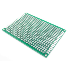
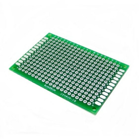
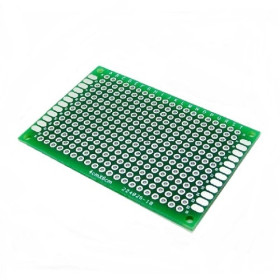
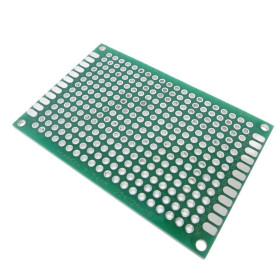
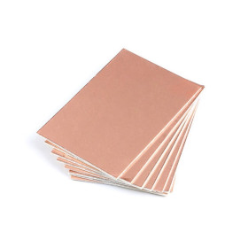
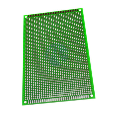
Prototyping PCB, 9 x 15 cm, single-sided, FR4, 2.54 mm pitch
Ideal for quickly building prototypes and electronic assemblies, this single-sided prototyping PCB provides a solid and reliable base for soldering and testing. Its 9 x 15 cm size suits medium-sized projects, it is made of durable FR4, and it offers mechanical stability and easy handling in the workshop or laboratory.
Buying this product earns you 0.52 RON in loyalty points.

International fast shipping within EU. Free Shipping for orders above 100 EUR in most EU countries.

We ship from our stock within 24H

You earn points with every order, worth 5%.
The single-sided copper-clad prototyping PCB is a universal support for soldering components with through-hole terminals. Resistors, capacitors, LEDs, DIP integrated circuits, connectors and pin modules are mounted on it, and an assembly built on it becomes a stable and durable circuit. It is suitable for prototypes, laboratory setups, school projects and small batches of hand-made circuits.
The board is made of FR4, a glass fibre laminate impregnated with epoxy resin, and measures 9 x 15 cm. The holes are arranged at the standard pitch of 2.54 mm (0.1 inch), the pitch used by DIP integrated circuits, pin headers and most connectors. Each hole has an individual copper pad around it, and the pads are not connected to each other. All circuit connections are made by soldering, with solder bridges or short wires.
The main features include the dense matrix of holes with individual pads, the rows of pads along the edges of the board, useful for power wires or connectors, and the 4 mounting holes in the corners for screws and spacers. The board contains no active components and has no power supply of its own, so it remains completely at the user's disposal for any schematic.
Specifications:
Board type: Prototyping, single-sided copper-clad
Material: FR4
Hole pitch: 2.54 mm
Mounting holes: 4, in the corners
Dimensions: 9 x 15 cm
Layout:
| Element | Function |
|---|---|
| Holes at 2.54 mm pitch | They receive the pin terminals of the components and form the soldering points of the circuit. |
| Individual pads | One copper pad around each hole, not connected to the neighbouring pads. Connections are made by soldering, with solder bridges or wires. |
| Pads on the board edges | Connection points for power wires or connectors soldered by the user. |
| Corner mounting holes | Fixing the board in a housing or on a support, with screws and spacers. |
Usage:
Set the placement of the components before soldering, on the side without copper, and leave at least one free hole between large components.
Insert the component terminals into the holes, turn the board over onto the copper side and bend the terminals slightly outwards so that the part does not fall out.
Heat the pad and the terminal at the same time for 1 - 2 seconds, then bring the solder to the contact point, not to the tip of the iron. A correct joint forms a shiny cone that covers the pad.
Do not move the part until the joint has cooled, to avoid cold joints, which are dull and brittle.
Make the connections between pads with solder bridges or short wires, because the board does not have ready-made tracks.
Cut off the terminals that stick out too much after the joint has cooled, leaving 1 - 2 mm above the solder.
Limit the contact of the iron with a pad to a few seconds and avoid repeatedly desoldering the same component, because the pad may come off the board.
Do not force thick terminals into the holes. File them down slightly or use a short wire between the part and the board.
Before powering up, check with the multimeter on the continuity setting that there is no short circuit between plus and minus and that every connection of the schematic is made.
Power the circuit respecting the voltage and polarity required by the soldered components, because the board itself does not limit or protect anything.
Fix the board in the housing or on the support with screws and spacers through the corner holes.
- Dimensions
- 9 x 15 cm
- Material
- FR4
- Type
- Single-sided prototyping board
- Pin pitch
- 2.54 mm
Produs destinat utilizarii in proiecte electronice, automatizari, prototipare, educatie si cercetare.
Produsul trebuie utilizat numai conform specificatiilor tehnice mentionate in descriere si/sau in documentatia produsului.
Avertismente generale de siguranta:
Nu utilizati produsul la tensiuni, curenti sau temperaturi peste valorile specificate.
Montajul si conectarea trebuie realizate de persoane cu cunostinte tehnice minime in domeniul electric/electronic.
Evitati scurtcircuitele, inversarea polaritatii si conectarea gresita a alimentarii.
Nu lasati produsul alimentat nesupravegheat in timpul testelor.
Produsul nu este jucarie si nu este destinat copiilor.
Pentru modulele electronice, se recomanda utilizarea in carcase, panouri sau montaje protejate, dupa caz.
Identificare produs:
Denumirea produsului, codul/SKU-ul si caracteristicile tehnice sunt mentionate in pagina produsului si/sau pe eticheta ambalajului.
Producator / Importator / Distribuitor:
Sigmanortec S.R.L.
Calea Bucuresti nr. 9, Targu Jiu, Gorj, Romania
E-mail: [email protected]
Website: www.sigmanortec.ro
Persoana responsabila in UE:
Sigmanortec S.R.L.
Calea Bucuresti nr. 9, Targu Jiu, Gorj, Romania
E-mail: [email protected]
Documentatie si siguranta:
Pentru informatii suplimentare, fise tehnice, declaratii de conformitate sau instructiuni, ne puteti contacta la [email protected].
Reviews (7) - Review moderation

Foarte bun
cele mai bune preturi de pe piata,la acelasi nivel de calitate
Ok
IDEALA
Ok
The 9 x 15 cm prototyping PCB is a universal FR4 board with single-sided copper and holes at the standard 2.54 mm pitch. You solder through-hole components onto it, from resistors and LEDs to DIP integrated circuits, connectors and pin-header modules, to turn a breadboard circuit into a stable one.
The board has no controller, it is not powered and it is not programmed. The tutorial uses a simple circuit powered from a 5 VDC source, with no program and no development board. It shows step by step how to place and solder the components and how to check the assembly.

How it works:
The board is a sheet of FR4, a fiberglass laminate impregnated with epoxy resin, with copper on one side only. Individual pads are formed in the copper around each hole. The pads are not connected to each other, so the board does not contain any ready-made connection. You create every connection in the circuit yourself, with a drop of solder, a short wire or a solder bridge between neighboring pads.
The distance between holes is 2.54 mm, or 0.1 inch. This is the pitch used by the legs of DIP integrated circuits, pin headers, connectors and most modules for makers, so they fit directly into the holes. Between the two rows of legs of a narrow DIP circuit the distance is 7.62 mm, or 3 steps.
For the 9 x 15 cm size, calculating the number of positions is simple: 90 / 2.54 = 35.4 and 150 / 2.54 = 59.1. On the two sides there is room for at most 35 and 59 holes respectively, and the actual number is slightly smaller because of the edges and the mounting holes in the corners. Use these values to plan the layout before soldering.
Connection:
The board has no signal pins and does not connect to any power source by itself. The test circuit in the tutorial is a red LED powered from a 5 VDC 1 A mains adapter, with the output brought out to a 5.5 x 2.1 mm jack adapter with screw terminals. The supply voltage is 5 V, logic levels do not play a role, and no level shifter or pull-up resistors are needed. Plug the adapter into the mains only after the assembly is finished and checked.
| Board pin | Connect to | Role |
|---|---|---|
| Pad where the first terminal of the 330 ohm resistor R1 is soldered | The + terminal of the jack adapter, using a short wire | Brings the 5 V positive to the resistor |
| Pad of the second terminal of R1 and pad of the LED anode (long leg) | Solder bridge or short wire between the two pads | Connects the resistor to the anode of the 5 mm red LED |
| Pad of the LED cathode (short leg, flat side) | The - terminal of the jack adapter, using a short wire | Closes the circuit to ground |
| Mounting holes in the corners | Screws and spacers | Fixes the board in an enclosure or on a support |
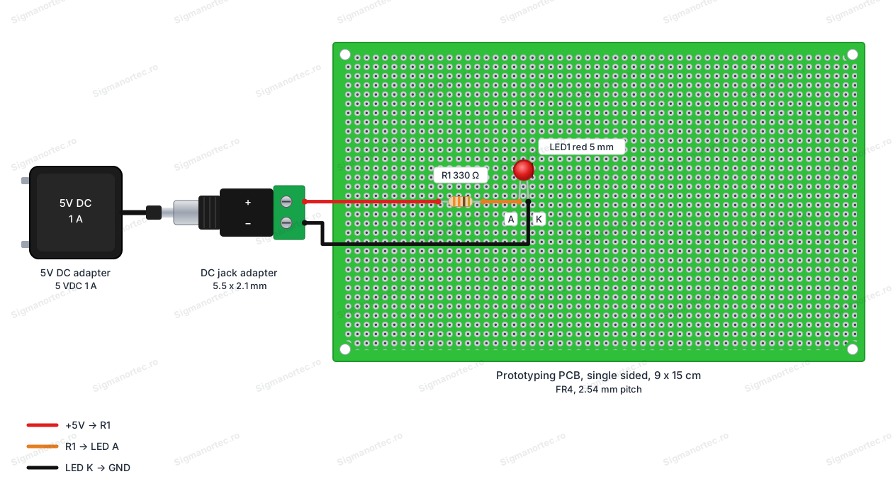
The board itself does not limit or protect anything. Respect the voltage and polarity required by the soldered components.
Usage example:
The example is a simple test circuit, a red LED powered from 5 V through a resistor. It is enough to practice all the steps: placing, soldering, cutting and checking. A red LED has a forward voltage of about 2 V. For a desired current of 10 mA, the resistor is calculated as follows: R = (5 V - 2 V) / 0.01 A = 300 ohm. The nearest standard value is 330 ohm, and the actual current becomes (5 - 2) / 330 = 9.1 mA. The power dissipated by the resistor is 3 V x 9.1 mA = 0.03 W, so a 1/4 W resistor has a large margin.
Step 1: decide the layout. Place the components on the board, on the side without copper, and settle their positions. Leave at least one free hole between the large components and keep a corner or an edge for the supply wires.
Step 2: fix the first component. Insert the 330 ohm resistor into two holes at a suitable distance, then turn the board over to the copper side. Gently bend the terminals outward so the part does not fall out.
Step 3: solder. Heat the pad and the terminal together for 1 - 2 seconds, then bring the solder to the contact point, not to the tip of the iron. Let the joint cool without moving the part. The solder should form a shiny cone that covers the pad.
Step 4: add the LED. The longer leg of the LED is the anode and is connected toward the resistor. The short leg, next to the flat side, is the cathode and is connected toward the negative. Mount the LED in the next row of holes and solder it as in step 3.
Step 5: make the connections. The free terminal of the resistor and the LED anode are on different pads, so join them with a solder bridge or a short wire. Then solder two supply wires, positive to the resistor and negative to the LED cathode, and connect them to the terminals of the jack adapter.
Step 6: cut the terminals that stick out too far, using flush cutters, after the joint has cooled. Leave 1 - 2 mm above the solder.
Step 7: check before powering. With the multimeter set to continuity, verify that there is no short circuit between positive and negative. Then power the assembly from the 5 VDC adapter. The LED should light up steadily. If it does not light, disconnect the power, check the solder joints and the orientation of the LED, because it is most likely mounted backwards.
Common problems:
An unwanted solder bridge appears between two neighboring pads. The cause is too much solder or the small spacing between holes. The fix is to heat the bridge and remove it with desoldering braid, then check with the multimeter that the two pads no longer have continuity.
The solder joint is dull and the part moves slightly. This is a cold joint, made with too low a temperature or with the part moved while it cooled. Heat the point again, add a little fresh solder and keep the part still until it solidifies.
A pad lifts off the board. The cause is heating for too long or desoldering the same component repeatedly. Limit the iron contact to a few seconds and, if the pad has come off, connect the terminal to a neighboring pad with a short wire.
A component terminal does not fit into the hole. The cause is a terminal that is too thick or a part with a pitch other than 2.54 mm. Lightly thin the terminal with a file, or use a short wire between the part and the board instead of forcing the terminal, because forcing it can tear off the pad.
The circuit does not work even though the components look correctly soldered. The usual cause is that two points that should be connected have no connection, since the board has no ready-made traces. Use the multimeter in continuity mode to check every connection in the schematic.
Limitations and tips:
The board has copper on one side only, so the pads and the solder joints are on the same side, and the components are mounted on the opposite side. Connections between pads must be made with solder or wires, which limits the complexity of the circuits you can build.
The board has no power traces and no protection. For higher currents, use wires of a suitable gauge instead of thin solder bridges, and keep the power connections as short as possible.
Plan the layout before soldering, keeping in mind that at most 35 x 59 holes fit on 9 x 15 cm. Group the components into functional blocks and leave the edges free for connectors and wires.
With this board you can go on to build permanent assemblies with several DIP integrated circuits, power distribution boards, adapters for pin-header modules and test circuits with many components.