
Product images are for informational purposes only and may vary slightly depending on the batch and supplier. Product specifications and prices may be subject to change without notice. We do our best to provide accurate and complete product specifications, but they may not be completely accurate. If you encounter any such situation, please let us know.
The product is intended for specialists and requires qualified and authorized personnel. The product does not include assembly/use instructions . Putting the product into operation by unqualified persons leads to the loss of the warranty according to the Terms and Conditions on the site.
The specified technical parameters (current, power, etc.) represent maximum allowable values under ideal operating conditions. For safe use and optimal lifespan, it is recommended to operate the product continuously at no more than 50% of the specified maximum values.
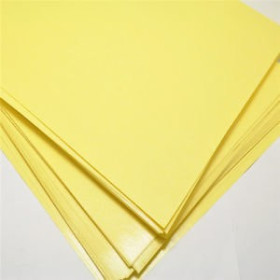
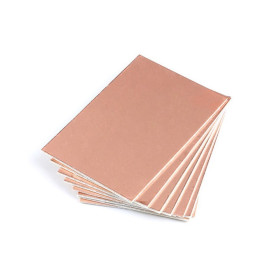
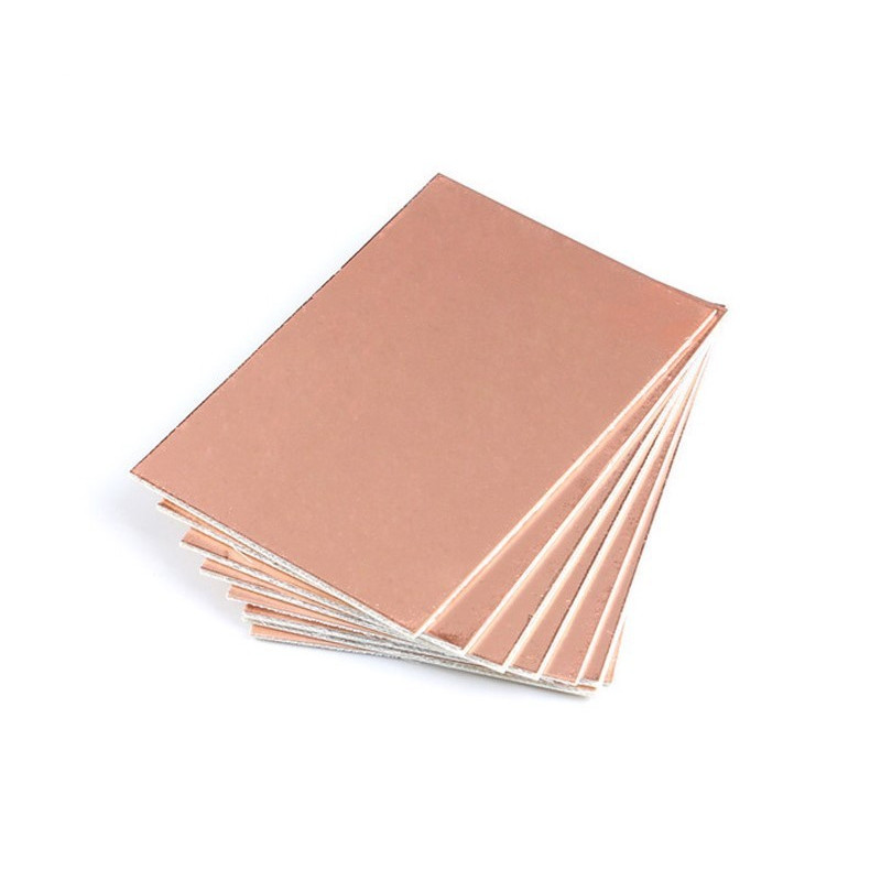
Laminated copper PCB board 10x15cm, single-sided copper
The laminated copper PCB board is ideal for quickly making printed circuits by etching or engraving. It measures 10x15 cm, with a uniform copper surface for precise transfer, single-sided construction for simple projects and prototypes, and rigid material that is easy to machine and cut as needed.
Shipping by Wednesday 11 November
Buying this product earns you 0.46 RON in loyalty points.

International fast shipping within EU. Free Shipping for orders above 100 EUR in most EU countries.

We ship from our stock within 24H

You earn points with every order, worth 5%.
Single-sided laminated copper PCB board is a blank for making your own printed circuit boards. From it you can obtain boards for prototypes, small modules, adapters and assemblies that are not available ready-made, by transferring the track pattern onto the copper and etching away the excess copper. It is suitable for laboratory, workshop, school and hobby projects.
The board measures 10 x 15 cm, that is an area of 150 cm2, and has a copper layer on one side only, the other side remaining insulating. The rigid material is easy to cut to the desired size, for example into two pieces of 10 x 7.5 cm or four pieces of 5 x 7.5 cm, so that a single board is enough for several small assemblies. The uniform copper surface allows precise transfer of the pattern by the toner transfer method, with marker, with photosensitive resist or by mechanical engraving.
Main characteristics include the single-sided copper layer, the 150 cm2 surface, the rigid material that is easy to cut and drill, and the fact that it is suitable for both chemical etching and milling. The board has no components and is not powered, the working voltage being that required by the circuit built on it.
Specifications:
Product type: Laminated copper PCB board
Copper sides: 1 (single side)
Surface: 150 cm2
Dimensions: 100 x 150 mm
Usage:
Draw the circuit in a design program on a single copper layer, with tracks wide enough and large distances between them, because tracks cannot cross on a single-sided board.
Cut the board to the size of the circuit with a fine-tooth metal saw or with tin snips, then file the edges and remove the burrs.
Clean the copper side with fine abrasive paper or an abrasive sponge, then wipe it with isopropyl alcohol, until the copper becomes shiny and free of grease marks.
Transfer the track pattern onto the copper, for example with toner from a laser printer, with permanent marker, with photosensitive resist or by mechanical engraving. For toner transfer, print the pattern mirrored.
Etch the board in a ferric chloride or sodium persulfate solution, in a plastic or glass container, with the copper facing up, and take it out as soon as all the unprotected copper has disappeared.
Use gloves and protective goggles, because etching solutions burn the skin and stain clothes, and do not pour the used solution down the drain.
Rinse the board with water, remove the protection with acetone or alcohol, drill the pads with a 0.8 - 1 mm drill bit from the copper side, then solder the components on the track side.
Before powering the finished circuit, check with a multimeter on the continuity setting that the tracks are not broken and that there are no short circuits, and to protect the copper against oxidation, apply a thin layer of flux or solder mask lacquer.
- Dimensions
- 100 x 150 mm
- Type
- Copper clad PCB board
Produs destinat utilizarii in proiecte electronice, automatizari, prototipare, educatie si cercetare.
Produsul trebuie utilizat numai conform specificatiilor tehnice mentionate in descriere si/sau in documentatia produsului.
Avertismente generale de siguranta:
Nu utilizati produsul la tensiuni, curenti sau temperaturi peste valorile specificate.
Montajul si conectarea trebuie realizate de persoane cu cunostinte tehnice minime in domeniul electric/electronic.
Evitati scurtcircuitele, inversarea polaritatii si conectarea gresita a alimentarii.
Nu lasati produsul alimentat nesupravegheat in timpul testelor.
Produsul nu este jucarie si nu este destinat copiilor.
Pentru modulele electronice, se recomanda utilizarea in carcase, panouri sau montaje protejate, dupa caz.
Identificare produs:
Denumirea produsului, codul/SKU-ul si caracteristicile tehnice sunt mentionate in pagina produsului si/sau pe eticheta ambalajului.
Producator / Importator / Distribuitor:
Sigmanortec S.R.L.
Calea Bucuresti nr. 9, Targu Jiu, Gorj, Romania
E-mail: [email protected]
Website: www.sigmanortec.ro
Persoana responsabila in UE:
Sigmanortec S.R.L.
Calea Bucuresti nr. 9, Targu Jiu, Gorj, Romania
E-mail: [email protected]
Documentatie si siguranta:
Pentru informatii suplimentare, fise tehnice, declaratii de conformitate sau instructiuni, ne puteti contacta la [email protected].
Reviews (3) - Review moderation

Super
Buna placa,dar e putin cam groasa (1,5mm) ar fi potrivita pentru montaje cu tuburi electronice !
Recomand
The 10x15cm PCB laminate board is a blank for printed circuit boards, copper-clad on one side only. You use it to make your own boards for prototypes, small modules, adapters or setups that are not available ready-made. It is a material, not an electronic module, so this tutorial explains step by step how to make a printed circuit from it, without a development board and without a program.
After etching, the side covered with copper becomes the network of tracks that connects the components. The side without copper remains insulated and receives the components with their terminals, which are soldered on the track side.
How it works:
The board consists of a rigid insulating base and a layer of copper on one side only. The printed circuit is obtained by the subtractive method: you cover only the copper areas that must remain with a protective resist, and dissolve the rest of the copper in an etching solution. The tracks stay under the protection, while the exposed areas become insulated surfaces.
The size of 10 x 15 cm means an area of 10 x 15 = 150 cm2. The board can be divided as needed, for example into two pieces of 10 x 7.5 cm (75 cm2 each) or into four pieces of 5 x 7.5 cm (37.5 cm2 each). In this way, a single board is enough for several small projects.
Because the copper is on one side only, the tracks cannot cross each other. When the layout requires a crossing, use an insulated wire jumper on the component side or rearrange the placement of the parts.
Connecting:
The board has no pins, it is not powered and it does not connect to anything in the form in which it is delivered. Power and connections appear only after you have made the circuit and soldered the components onto it, and the correct voltage is the one required by the circuit you have built.
Configuration:
Step 1. Design the circuit in a schematic and board layout program, for example KiCad or EasyEDA, on a single copper layer. Choose wide tracks and large distances between them, because a simple trace etches more easily and with fewer errors.
Step 2. Cut the board to the size of the circuit. Mark the line with a cutter or a marker, then cut with a fine metal saw or tin snips. Sand the edges and remove any burrs.
Step 3. Clean the copper side. Gently rub the surface with fine abrasive paper or an abrasive sponge, then wipe it with isopropyl alcohol. The copper must be shiny and free of grease marks, because fingerprints and oxide prevent both the transfer of the pattern and uniform etching.
Step 4. Transfer the track pattern onto the copper using one of the methods in the table. With the toner transfer method, the laser printer prints the pattern mirrored, so that after soldering you get the correct orientation when viewed from the component side.
| Method | How it is done | Suitable for |
|---|---|---|
| Toner transfer | Print the pattern mirrored with a laser printer on glossy paper, press the paper onto the copper with a clothes iron or with a laminator, and remove the paper after cooling and soaking in water. | Circuits with fine, repeatable tracks |
| Permanent marker | Draw the tracks and pads directly with a marker that is resistant to water and etching. | Simple setups, made only once |
| Photosensitive resist | Coat the copper with photosensitive resist, expose to UV through a printed film and develop. | Dense circuits, with several copies |
| CNC engraving | Mechanically remove the copper between the tracks with an engraving cutter. | Prototypes without chemicals |
Step 5. Etch the board. Prepare a solution of ferric chloride or sodium persulfate in a plastic or glass container, never a metal one. Immerse the board with the copper facing up and gently move the container. Etching goes faster with a slightly warmed and agitated solution. Remove the board as soon as all the unprotected copper has disappeared.
Step 6. Rinse the board with water and remove the protection. Toner is cleaned off with acetone or thinner, and marker with alcohol. Wear gloves and protective goggles, because etching solutions burn the skin and stain clothes. Do not pour the used solution down the drain.
Step 7. Drill the pads for the component terminals. Choose the drill bit according to the thickness of the terminals, usually around 0.8 - 1 mm for resistors, capacitors and integrated circuits. Drill with the copper side facing up, at high speed and with light pressure, so that the copper does not lift around the hole.
Step 8. Protect the tracks. A thin layer of flux or solder mask lacquer prevents the copper from oxidizing and makes soldering easier. Before soldering, clean the pads again with a fine abrasive sponge.
Usage example:
The example builds a small 5 V regulator with the 7805 circuit, on a piece of board cut to 5 x 7.5 cm, which is a quarter of the board. The setup has an input connector, an output connector, the 7805 circuit and two filter capacitors.
Draw a single copper side, with the input on the left and the output on the right. Print the pattern mirrored on glossy paper, transfer it onto the cleaned copper and etch the board until all the exposed copper has disappeared. Remove the toner, drill the pads with a 0.8 mm drill bit and solder the components onto the copper side, after inserting them from the side without copper.
Before powering up, check with a multimeter on the continuity setting that the tracks are not broken and that there is no short circuit between the input and ground. Then power the input with 9 VDC, with the correct polarity. The expected result is a voltage of about 5 V measured at the output, relative to ground.
Common problems:
The toner does not transfer completely onto the copper. The usual cause is dirty copper or a temperature that is too low during transfer. Clean the surface again with isopropyl alcohol and press the paper for longer, with even heat.
The tracks are thinned or broken after etching. The board stayed too long in the solution or the protection had small gaps. Monitor the board during etching, remove it as soon as the unprotected copper has disappeared and touch up the gaps with marker before etching.
Etching is very slow or uneven. The solution is old, cold or was not agitated. Use fresh solution, slightly warmed, and gently move the container for the entire duration of the etching.
The copper lifts around the holes when drilling. The drill bit is blunt or the pressure is too high. Use a sharp drill bit, high speed and light pressure, with the copper side facing up.
The solder does not stick to the pads. The copper has oxidized after etching. Clean the pads with a fine abrasive sponge just before soldering and apply flux.
Limitations and tips:
The board has copper on one side only, so complex circuits with many track crossings require wire jumpers or a double-sided board. The precision of the tracks depends on the transfer method and the cleanliness of the copper, and very fine tracks are harder to achieve with a marker.
For tracks that carry high currents, draw them wider and check after etching that there are no thinned areas. Keep the unused board away from moisture, because copper oxidizes over time, and clean it again before use.
A 10 x 15 cm board can be divided into several pieces, so you can build several small setups one after another, from regulators and adapters to small signal circuits.