Product images are for informational purposes only and may vary slightly depending on the batch and supplier. Product specifications and prices may be subject to change without notice. We do our best to provide accurate and complete product specifications, but they may not be completely accurate. If you encounter any such situation, please let us know.
The product is intended for specialists and requires qualified and authorized personnel. The product does not include assembly/use instructions . Putting the product into operation by unqualified persons leads to the loss of the warranty according to the Terms and Conditions on the site.
The specified technical parameters (current, power, etc.) represent maximum allowable values under ideal operating conditions. For safe use and optimal lifespan, it is recommended to operate the product continuously at no more than 50% of the specified maximum values.
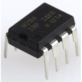
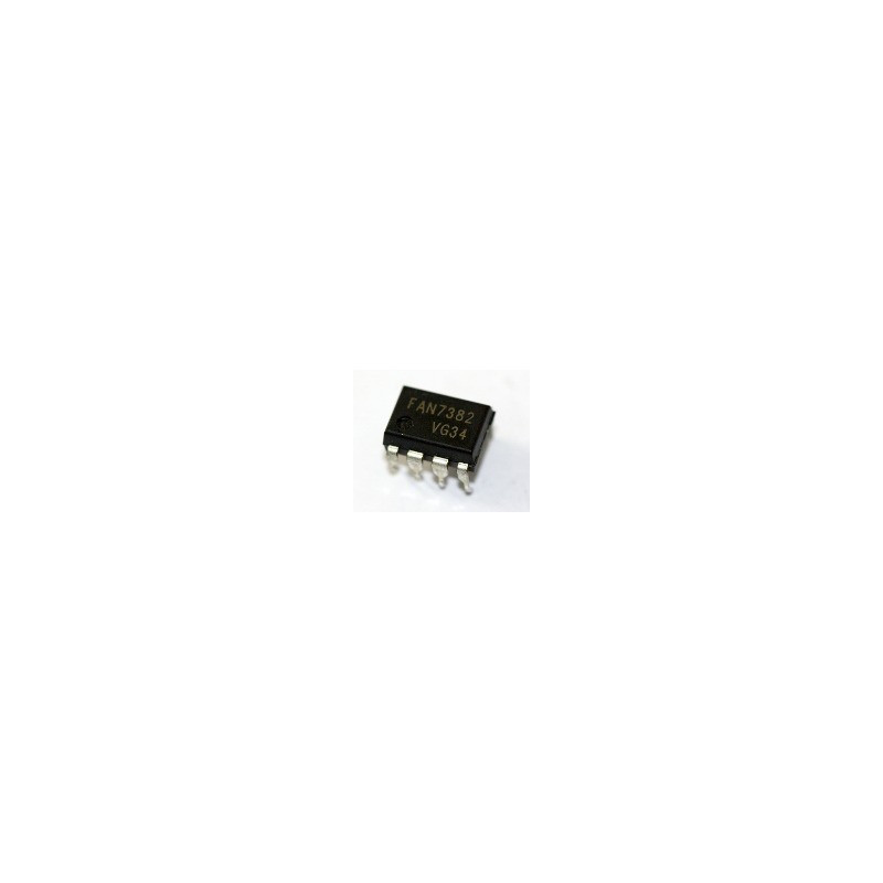
FAN7382 Half-Bridge Gate Driver, up to 600V, 350mA / 650mA, DIP-8
Monolithic half-bridge driver for fast and reliable control of MOSFETs and IGBTs in power applications, supporting operating voltages up to 600V, integrated in a single package for a compact and reliable design, compatible with common logic levels, with UVLO protection for stable operation, available in DIP-8 for easy mounting.
Shipping by Wednesday 11 November
Buying this product earns you 0.57 RON in loyalty points.

International fast shipping within EU. Free Shipping for orders above 100 EUR in most EU countries.

We ship from our stock within 24H

You earn points with every order, worth 5%.
FAN7382 is a monolithic half-bridge gate driver with two control channels, one for the high-side transistor and one for the low-side transistor. The circuit receives low-level logic signals and drives N-channel MOSFETs and IGBTs operating at voltages up to 600 V. It is suitable for switching power supplies, converters, inverters, motor control and fluorescent lamp ballasts.
The high-side channel is floating and is powered in bootstrap mode, with a capacitor connected between VB and VS. Each channel typically provides 350 mA when turning the transistor on and 650 mA when turning it off. The circuit is powered with 10 - 20 V on VCC and VBS and has UVLO protection on both channels, with a typical turn-on threshold of 9.2 V. The HIN and LIN inputs are TTL compatible, so above 2.9 V they are interpreted as logic 1, and below 0.8 V as logic 0. The HO and LO outputs are in phase with the inputs. The propagation delays of the two channels are matched to a maximum difference of 50 ns. The common-mode dv/dt noise cancellation circuit keeps the high-side drive stable, and a level shifter stage allows operation with a negative VS voltage of up to -9.8 V typical.
Main features include the DIP-8 package with 2.54 mm pitch, suitable for breadboards and through-hole PCBs, two independent logic inputs HIN and LIN, outputs HO and LO for the transistor gates, pins VB and VS for the bootstrap capacitor, and the common COM pin for logic ground and the low-side return. Power is supplied with 10 - 20 V on the VCC pin, and the high-side channel receives energy through the bootstrap capacitor and an external fast diode.
The HIN and LIN inputs can be driven directly from the digital or PWM outputs of an Arduino Uno board, which has 5 V logic, or from any other microcontroller with TTL compatible outputs.
Specifications:
VCC supply voltage: 10 - 20 VDC
Gate output current (source / sink): 350 mA / 650 mA typical, per channel
Circuit type: Half-bridge gate driver, high-side and low-side
Controlled transistors: N-channel MOSFET and IGBT
Maximum half-bridge voltage (VS): 600 V
High-side supply: Bootstrap, VBS 10 - 20 V
Number of channels: 2, independent
Input logic level (HIN, LIN): TTL, logic 1 above 2.9 V, logic 0 below 0.8 V
Output polarity: In phase with the inputs
UVLO threshold VCC and VBS: 9.2 V turn-on, 8.7 V turn-off (typical)
Output rise / fall time: 60 ns / 30 ns typical (1000 pF load)
Propagation delay: 170 ns turn-on, 200 ns turn-off (typical)
Channel mismatch: maximum 50 ns
VCC quiescent current: 70 uA typical
Allowed negative VS voltage: -9.8 V typical
Operating temperature: -40 - 125 °C
Package: DIP-8, 2.54 mm pitch
Dimensions: 9.2 x 6.4 mm
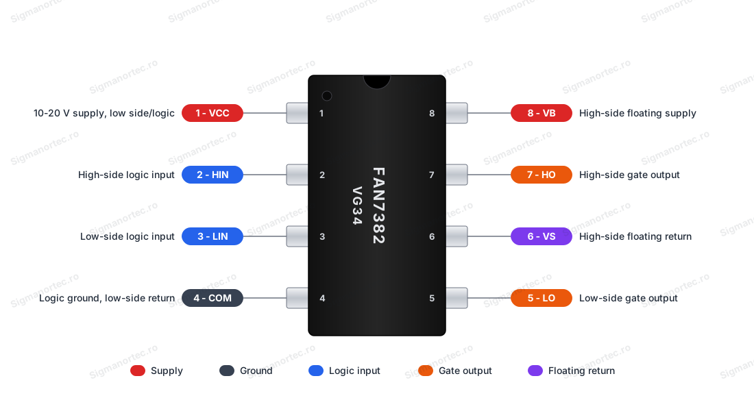
Pinout:
| Connector | Pin | Function |
|---|---|---|
| DIP-8 | 1 - VCC | Power supply for the low-side channel and for the logic, 10 - 20 V |
| DIP-8 | 2 - HIN | Logic input for the high-side output HO |
| DIP-8 | 3 - LIN | Logic input for the low-side output LO |
| DIP-8 | 4 - COM | Logic ground and return of the low-side driver |
| DIP-8 | 5 - LO | Low-side driver output, connects to the gate of the low-side transistor |
| DIP-8 | 6 - VS | Return of the floating supply, connects to the middle of the half-bridge |
| DIP-8 | 7 - HO | High-side driver output, connects to the gate of the high-side transistor |
| DIP-8 | 8 - VB | Floating supply of the high-side channel, to the bootstrap capacitor |
Usage:
Voltages up to 600 V are dangerous. Make the connections only with the assembly disconnected from the power supply, and perform the first test with a low voltage bus, for example 12 V.
Supply the VCC pin with 10 - 20 V relative to COM and place a 100 nF ceramic capacitor and a 10 uF electrolytic capacitor close to the pins.
Connect a fast diode between VCC and VB, with the anode at VCC, and a bootstrap capacitor between VB and VS. The diode must withstand the power bus voltage.
Connect the VS pin to the middle of the half-bridge, that is, to the source of the high-side transistor and the drain of the low-side transistor.
Connect the HO and LO outputs to the transistor gates through series resistors of 10 - 47 ohms, which limit the gate charging current and oscillations.
Connect the COM pin to the control signal ground, the supply ground and the source of the low-side transistor.
Drive HIN and LIN with logic signals of logic 1 above 2.9 V and logic 0 below 0.8 V, and make sure the logic 1 level does not exceed the VCC voltage.
Before the first high-side command, briefly activate LIN to charge the bootstrap capacitor, because during this time VS is pulled close to ground.
Do not drive HIN and LIN simultaneously at logic 1. The two channels are independent, so the dead time between switchings must be generated by the control signal.
For stable results, keep the traces between the driver and the transistor gates as short as possible and decouple VCC with capacitors placed right next to the circuit.
- Supply voltage
- 10-20 V DC
- Dimensions
- 9.2 x 6.4 mm
- Type
- Half-bridge gate driver, high-side and low-side
- Operating temperature
- -40-125 °C
- Output current
- 350 mA / 650 mA
- Logic voltage
- TTL, level 1 above 2.9 V, level 0 below 0.8 V
- Number of channels
- 2, independente
- Maximum voltage
- 600 V
- Integrated circuit
- FAN7382
- Pin pitch
- 2.54 mm
- Package
- DIP-8, 2.54 mm pitch
- No-load current
- 70 µA
Produs destinat utilizarii in proiecte electronice, automatizari, prototipare, educatie si cercetare.
Produsul trebuie utilizat numai conform specificatiilor tehnice mentionate in descriere si/sau in documentatia produsului.
Avertismente generale de siguranta:
Nu utilizati produsul la tensiuni, curenti sau temperaturi peste valorile specificate.
Montajul si conectarea trebuie realizate de persoane cu cunostinte tehnice minime in domeniul electric/electronic.
Evitati scurtcircuitele, inversarea polaritatii si conectarea gresita a alimentarii.
Nu lasati produsul alimentat nesupravegheat in timpul testelor.
Produsul nu este jucarie si nu este destinat copiilor.
Pentru modulele electronice, se recomanda utilizarea in carcase, panouri sau montaje protejate, dupa caz.
Identificare produs:
Denumirea produsului, codul/SKU-ul si caracteristicile tehnice sunt mentionate in pagina produsului si/sau pe eticheta ambalajului.
Producator / Importator / Distribuitor:
Sigmanortec S.R.L.
Calea Bucuresti nr. 9, Targu Jiu, Gorj, Romania
E-mail: [email protected]
Website: www.sigmanortec.ro
Persoana responsabila in UE:
Sigmanortec S.R.L.
Calea Bucuresti nr. 9, Targu Jiu, Gorj, Romania
E-mail: [email protected]
Documentatie si siguranta:
Pentru informatii suplimentare, fise tehnice, declaratii de conformitate sau instructiuni, ne puteti contacta la [email protected].
/*
  FAN7382 half-bridge gate driver test
  Board: Arduino Uno (Tools > Board > Arduino AVR Boards > Arduino Uno)
  Board package: Arduino AVR Boards (Boards Manager)
  Libraries: none, only the core Arduino functions are used

  Wiring:
    FAN7382 pin 1 VCC -> +12 V (with 100 nF and 10 uF to COM, bootstrap diode anode)
    FAN7382 pin 2 HIN -> Arduino D9
    FAN7382 pin 3 LIN -> Arduino D10
    FAN7382 pin 4 COM -> Arduino GND, supply GND, low-side MOSFET source
    FAN7382 pin 5 LO  -> low-side MOSFET gate (series resistor)
    FAN7382 pin 6 VS  -> half-bridge midpoint, bootstrap capacitor minus
    FAN7382 pin 7 HO  -> high-side MOSFET gate (series resistor)
    FAN7382 pin 8 VB  -> bootstrap diode cathode, bootstrap capacitor plus

  Test first at a low bus voltage (12 V), never at 600 V.
*/

const uint8_t HIN_PIN = 9;                 // Input of the high-side driver
const uint8_t LIN_PIN = 10;                // Input of the low-side driver

const unsigned int HIGH_ON_US = 40;        // High-side on time in microseconds
const unsigned int LOW_ON_US = 40;         // Low-side on time in microseconds
const unsigned int DEAD_US = 5;            // Dead time between the two switches
const unsigned int BOOT_CHARGE_MS = 10;    // Low-side on time that charges the bootstrap capacitor

void setup() {
  Serial.begin(9600);                      // Start the serial monitor at 9600 baud

  pinMode(HIN_PIN, OUTPUT);                // Configure the control pins as outputs
  pinMode(LIN_PIN, OUTPUT);
  digitalWrite(HIN_PIN, LOW);              // Start with both switches off
  digitalWrite(LIN_PIN, LOW);

  Serial.println(F("FAN7382 half-bridge test"));

  // Turn the low side on to charge the bootstrap capacitor
  digitalWrite(LIN_PIN, HIGH);
  delay(BOOT_CHARGE_MS);
  digitalWrite(LIN_PIN, LOW);
  Serial.print(F("Bootstrap capacitor charged for "));
  Serial.print(BOOT_CHARGE_MS);
  Serial.println(F(" ms"));

  // Compute the nominal period and frequency without the digitalWrite overhead
  unsigned long periodUs = (unsigned long)HIGH_ON_US + LOW_ON_US + 2UL * DEAD_US;
  Serial.print(F("Nominal period: "));
  Serial.print(periodUs);
  Serial.println(F(" us"));
  Serial.print(F("Nominal frequency: "));
  Serial.print(1000000UL / periodUs);
  Serial.println(F(" Hz"));
  Serial.print(F("Dead time: "));
  Serial.print(DEAD_US);
  Serial.println(F(" us"));
  Serial.println(F("Switching started"));
}

void loop() {
  // Low side off, wait for the dead time, then high side on
  digitalWrite(LIN_PIN, LOW);
  delayMicroseconds(DEAD_US);
  digitalWrite(HIN_PIN, HIGH);
  delayMicroseconds(HIGH_ON_US);

  // High side off, wait for the dead time, then low side on
  digitalWrite(HIN_PIN, LOW);
  delayMicroseconds(DEAD_US);
  digitalWrite(LIN_PIN, HIGH);
  delayMicroseconds(LOW_ON_US);
}
In this tutorial we put the FAN7382 circuit into operation, a gate driver for a half bridge that controls two power transistors, one on the high side and one on the low side. It is used in switching power supplies, inverters, DC-DC converters and motor drivers, where a small logic signal must control transistors operating at high voltages.
The circuit does not generate the control signals on its own, so we need a microcontroller. We use an Arduino Uno board, which has digital outputs with 5 V logic, sufficient for the TTL inputs of the driver. The Arduino Uno is the simplest choice for this circuit, because it requires neither WiFi, nor additional memory, nor a special interface.
How it works:
The driver has two logic inputs, HIN and LIN, and two outputs, HO and LO, in phase with the inputs. Logic level 1 is considered above 2.9 V, and logic level 0 below 0.8 V. The LO output drives the gate of the low-side transistor, and the HO output drives the gate of the high-side transistor. Each channel typically supplies 350 mA when turning on and 650 mA when turning off.
The source of the high-side transistor sits at the middle of the half bridge, which rises and falls between ground and the bus voltage. That is why the supply of the high-side channel must follow this point. It is obtained with a bootstrap capacitor connected between VB and VS. When the low-side transistor is on, VS is pulled close to ground, and the capacitor charges from VCC through a fast diode. The high-side channel voltage is approximately VBS = VCC - VF, where VF is the voltage drop across the diode. For VCC = 12 V and VF = 0.7 V, VBS is about 11.3 V, above the typical 9.2 V UVLO turn-on threshold.
The switching speed depends on the gate charge Qg of the transistor and the driver current, according to the relation t = Qg / I. For a transistor with Qg = 30 nC, at 350 mA this gives about 86 ns on turn-on, and at 650 mA about 46 ns on turn-off. In reality the times are longer, because as the gate charges, the current decreases.
The signal generated by the program has the period T = tHigh + tDead + tLow + tDead. With 40 us, 5 us, 40 us and 5 us this gives 90 us, that is about 11.1 kHz, to which the time of the digitalWrite instructions is added. The dead time prevents both transistors from conducting at the same time, which would short-circuit the bus.
Connection:
For the first test use a 12 V power bus, not the maximum voltage of 600 V. High voltages are dangerous, so make the connections only with the setup disconnected. Power VCC with 12 V, within the range 10 - 20 V. The HIN and LIN inputs have TTL levels, so they connect directly to the Arduino Uno pins, without a level converter. The Arduino ground, the power supply ground and COM must be connected together. The transistors are two N-channel MOSFETs, and the load is connected between the middle of the half bridge and ground or the bus.
| Product pin | Connect to | Role |
|---|---|---|
| 1 - VCC | +12 V, anode of the bootstrap diode, 100 nF and 10 uF capacitors to COM | Supply for the low-side channel and for the logic. |
| 2 - HIN | Digital pin 9 on Arduino Uno | High-side channel control. |
| 3 - LIN | Digital pin 10 on Arduino Uno | Low-side channel control. |
| 4 - COM | Arduino GND, power supply GND, source of the low-side transistor | Common ground. |
| 5 - LO | Gate of the low-side transistor, through a series resistor of 10 - 47 ohms | Low-side driver output. |
| 6 - VS | Middle of the half bridge, negative terminal of the bootstrap capacitor | Return of the floating supply. |
| 7 - HO | Gate of the high-side transistor, through a series resistor of 10 - 47 ohms | High-side driver output. |
| 8 - VB | Cathode of the bootstrap diode, positive terminal of the bootstrap capacitor | Floating supply of the high-side channel. |
Board and libraries:
In the Arduino IDE select the Arduino Uno board at Tools > Board from the Arduino AVR Boards package, which is installed from the Boards Manager and usually comes with the Arduino IDE. The program uses only the basic functions of the platform, so no library needs to be installed.
The code:
The program briefly charges the bootstrap capacitor, then generates on pins 9 and 10 two complementary signals with dead time between them.
/*
  FAN7382 half-bridge gate driver test
  Board: Arduino Uno (Tools > Board > Arduino AVR Boards > Arduino Uno)
  Libraries: none, only the core Arduino functions are used
  Wiring:
    FAN7382 pin 1 VCC -> +12 V (with 100 nF and 10 uF to COM, bootstrap diode anode)
    FAN7382 pin 2 HIN -> Arduino D9
    FAN7382 pin 3 LIN -> Arduino D10
    FAN7382 pin 4 COM -> Arduino GND, supply GND, low-side MOSFET source
    FAN7382 pin 5 LO  -> low-side MOSFET gate (series resistor)
    FAN7382 pin 6 VS  -> half-bridge midpoint, bootstrap capacitor minus
    FAN7382 pin 7 HO  -> high-side MOSFET gate (series resistor)
    FAN7382 pin 8 VB  -> bootstrap diode cathode, bootstrap capacitor plus
  Test first at a low bus voltage (12 V), never at 600 V.
*/
const uint8_t HIN_PIN = 9;                 // Input of the high-side driver
const uint8_t LIN_PIN = 10;                // Input of the low-side driver
const unsigned int HIGH_ON_US = 40;        // High-side on time in microseconds
const unsigned int LOW_ON_US = 40;         // Low-side on time in microseconds
const unsigned int DEAD_US = 5;            // Dead time between the two switches
const unsigned int BOOT_CHARGE_MS = 10;    // Low-side on time that charges the bootstrap capacitor
void setup() {
  Serial.begin(9600);                      // Start the serial monitor at 9600 baud
  pinMode(HIN_PIN, OUTPUT);                // Configure the control pins as outputs
  pinMode(LIN_PIN, OUTPUT);
  digitalWrite(HIN_PIN, LOW);              // Start with both switches off
  digitalWrite(LIN_PIN, LOW);
  Serial.println(F("FAN7382 half-bridge test"));
  // Turn the low side on to charge the bootstrap capacitor
  digitalWrite(LIN_PIN, HIGH);
  delay(BOOT_CHARGE_MS);
  digitalWrite(LIN_PIN, LOW);
  Serial.print(F("Bootstrap capacitor charged for "));
  Serial.print(BOOT_CHARGE_MS);
  Serial.println(F(" ms"));
  // Compute the nominal period and frequency without the digitalWrite overhead
  unsigned long periodUs = (unsigned long)HIGH_ON_US + LOW_ON_US + 2UL * DEAD_US;
  Serial.print(F("Nominal period: "));
  Serial.print(periodUs);
  Serial.println(F(" us"));
  Serial.print(F("Nominal frequency: "));
  Serial.print(1000000UL / periodUs);
  Serial.println(F(" Hz"));
  Serial.print(F("Dead time: "));
  Serial.print(DEAD_US);
  Serial.println(F(" us"));
  Serial.println(F("Switching started"));
}
void loop() {
  // Low side off, wait for the dead time, then high side on
  digitalWrite(LIN_PIN, LOW);
  delayMicroseconds(DEAD_US);
  digitalWrite(HIN_PIN, HIGH);
  delayMicroseconds(HIGH_ON_US);
  // High side off, wait for the dead time, then low side on
  digitalWrite(HIN_PIN, LOW);
  delayMicroseconds(DEAD_US);
  digitalWrite(LIN_PIN, HIGH);
  delayMicroseconds(LOW_ON_US);
}
How the code works:
The constants HIN_PIN and LIN_PIN indicate pins 9 and 10, connected to the HIN and LIN inputs. The constants HIGH_ON_US, LOW_ON_US and DEAD_US set the conduction time of each transistor and the dead time, in microseconds. The constant BOOT_CHARGE_MS sets how long the low-side channel stays active to charge the bootstrap capacitor.
In the setup() function the serial monitor is started at 9600 baud, both pins are configured as outputs and set to LOW, so that both transistors start off. Then LIN is set to HIGH for BOOT_CHARGE_MS milliseconds, which charges the bootstrap capacitor, and returns to LOW. At the end the nominal period and frequency are calculated and displayed, in the variable periodUs.
The loop() function repeats the same sequence endlessly. First LIN is set to LOW, and the dead time is waited out. Then HIN is set to HIGH for HIGH_ON_US microseconds. After that HIN returns to LOW, the dead time is waited again, and LIN is set to HIGH for LOW_ON_US microseconds. At no moment are the two pins HIGH at the same time.
Result:
Open the serial monitor at 9600 baud. After resetting the board the startup messages appear, together with the bootstrap charging duration and the nominal values of the period and frequency. With an oscilloscope or logic analyzer on the HO and LO pins you see two complementary signals, with a pause of about 5 us between them.
FAN7382 half-bridge test
Bootstrap capacitor charged for 10 ms
Nominal period: 90 us
Nominal frequency: 11111 Hz
Dead time: 5 us
Switching started
Common problems:
The HO output does not switch. The most common cause is an uncharged bootstrap capacitor or a diode mounted backwards. Check that the diode has its anode at VCC and its cathode at VB, and that LO is activated long enough before the first HO command.
Both channels remain inactive. Check the VCC supply, which must be above the typical 9.2 V UVLO threshold, and check that the COM pin is connected to the Arduino ground. Without the common ground the logic levels are not recognized.
The transistors heat up strongly. They are possibly conducting at the same time. Check the HO and LO signals with the oscilloscope and increase the dead time DEAD_US until they no longer overlap.
Oscillations appear on the gates or the switching is erratic. Mount the 10 - 47 ohm series resistors as close as possible to the gates, shorten the traces and add the 100 nF capacitor directly between VCC and COM.
The high-side channel stops after a long conduction time. The bootstrap capacitor discharges gradually. Use continuous switching, with pauses in which the low-side transistor charges the capacitor again.
Limitations and tips:
The circuit has two independent channels and does not include internal protection against simultaneous conduction, so the dead time remains the responsibility of the control signal. Supplying the high-side channel through bootstrap requires periodic switching, so the high-side transistor cannot be kept on indefinitely.
The test program with digitalWrite reaches about 11 kHz and has small timing variations due to Arduino interrupts. For high frequencies and precise timing use the hardware timers of the microcontroller.
After the circuit works correctly at 12 V, the bus voltage can be increased gradually, with care for the dangerous voltages and with transistors rated for it. On this basis one can build a motor half bridge, a Buck converter or a complete bridge with two such drivers.