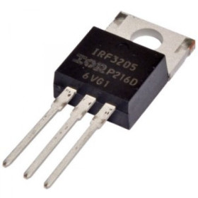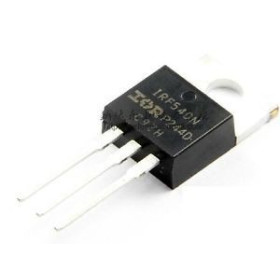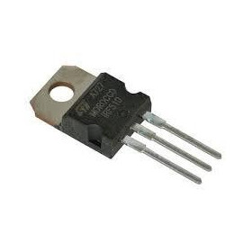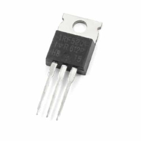

Product images are for informational purposes only and may vary slightly depending on the batch and supplier. Product specifications and prices may be subject to change without notice. We do our best to provide accurate and complete product specifications, but they may not be completely accurate. If you encounter any such situation, please let us know.
The product is intended for specialists and requires qualified and authorized personnel. The product does not include assembly/use instructions . Putting the product into operation by unqualified persons leads to the loss of the warranty according to the Terms and Conditions on the site.
The specified technical parameters (current, power, etc.) represent maximum allowable values under ideal operating conditions. For safe use and optimal lifespan, it is recommended to operate the product continuously at no more than 50% of the specified maximum values.
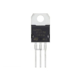
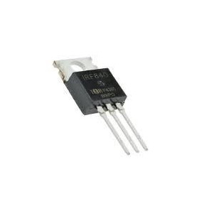
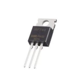
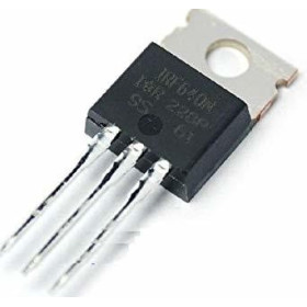
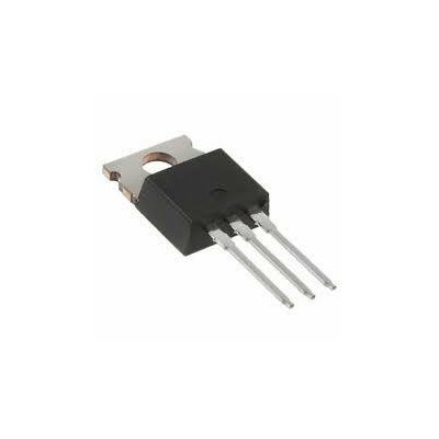
IRF830 N-Channel MOSFET Transistor, 500V, 4.5A, TO-220AB
N-Channel MOSFET for switching in switch-mode power supplies, inverters and industrial applications, withstands up to 500V VDS, offers low losses and fast switching, TO-220 package for easy heatsink mounting and efficient heat dissipation, suitable for power projects and electronics repairs.
Shipping by Wednesday 11 November
Buying this product earns you 0.18 RON in loyalty points.

International fast shipping within EU. Free Shipping for orders above 100 EUR in most EU countries.

We ship from our stock within 24H

You earn points with every order, worth 5%.
The IRF830 is an N-channel power MOSFET designed for switching DC loads at voltages up to 500 V. It is used as an electronic switch in switch-mode power supplies, in the control of motors and solid-state relays, and in circuits operating at high voltages, where a gate with simple drive requirements is needed.
The maximum drain-source voltage is 500 V, and the continuous drain current is 4.5 A at a case temperature of 25 °C and 2.9 A at 100 °C. The on-state resistance RDS(on) is at most 1.5 Ω, guaranteed at VGS = 10 V and ID = 2.7 A, so the gate must be driven with 10 - 12 V for full turn-on. The threshold voltage VGS(th) is between 2.0 and 4.0 V at ID = 250 µA, and the maximum gate-source voltage is ± 20 V. The input capacitance Ciss is approximately 610 pF, and the total gate charge is at most 38 nC.
The main features include the TO-220AB package with three terminals (gate G, drain D, source S), the metal tab electrically connected to the drain for mounting on a heatsink, the power dissipation of 74 W at a case temperature of 25 °C, the pulsed peak current of 18 A, and the operating temperature range from -55 to 150 °C.
Specifications:
Drain-source voltage (VDS): 500 V
Continuous drain current (ID): 4.5 A at TC = 25 °C, 2.9 A at TC = 100 °C
Pulsed drain current (IDM): 18 A
Type: N-channel power MOSFET
Maximum gate-source voltage (VGS): ± 20 V
Threshold voltage (VGS(th)): 2.0 - 4.0 V at ID = 250 µA
On-state resistance (RDS(on)): maximum 1.5 Ω at VGS = 10 V and ID = 2.7 A
Input capacitance (Ciss): 610 pF typical
Total gate charge (Qg): maximum 38 nC
Maximum power dissipation (PD): 74 W at TC = 25 °C
Thermal resistance junction-to-case: maximum 1.7 °C/W
Thermal resistance junction-to-ambient: maximum 62 °C/W
Operating temperature: from -55 to 150 °C
Package: TO-220AB, 3 terminals
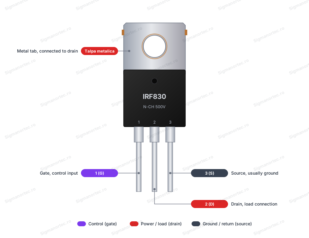
Pinout:
| Connector | Pin | Function |
|---|---|---|
| TO-220AB | 1 (G) | Gate, control input |
| TO-220AB | 2 (D) | Drain, the load is connected to it |
| TO-220AB | 3 (S) | Source, usually connected to circuit ground |
| TO-220AB | Metal tab | Electrically connected to the drain |
The pin numbering applies when looking at the transistor from the front, with the text side facing you and the pins pointing down, from left to right.
Usage:
Identify the pins looking at the transistor with the text side facing you and the pins down: 1 = G, 2 = D, 3 = S, from left to right.
Connect the load between the supply and the drain, and the source to circuit ground, so that the transistor switches the low side of the load.
Drive the gate with 10 - 12 V relative to the source, so that the on-state resistance reaches the guaranteed value. A 3.3 V or 5 V logic signal does not fully open the transistor, which remains partially on and heats up.
Do not apply gate voltages higher than ± 20 V relative to the source.
Fit a 47 - 470 Ω resistor in series with the gate, which limits the gate charging current, and a 10 - 100 kΩ resistor between the gate and the source, which discharges the gate and turns off the transistor when the drive is interrupted.
For inductive loads (motors, relays, coils), fit a protection diode in parallel with the load, with the cathode towards the plus and the anode towards the drain.
Check the load current. The conduction loss is P = I² × RDS(on), and for currents of around one ampere or more, use a heatsink.
Insulate the metal tab from the heatsink and from the chassis, because it is at drain potential, and do not touch it when the circuit is powered.
Handle the transistor with anti-static protection, and when soldering, do not exceed 300 °C for 10 s.
For testing, measure the drain-source voltage: with the gate driven, it should be a few tens of millivolts up to at most 0.15 V at 0.1 A, and with the gate at 0 V, it should be close to the load supply voltage.
- Type
- N-channel power MOSFET
- Operating temperature
- -55 la 150 °C
- Package
- TO-220AB, 3 terminale
Produs destinat utilizarii in proiecte electronice, automatizari, prototipare, educatie si cercetare.
Produsul trebuie utilizat numai conform specificatiilor tehnice mentionate in descriere si/sau in documentatia produsului.
Avertismente generale de siguranta:
Nu utilizati produsul la tensiuni, curenti sau temperaturi peste valorile specificate.
Montajul si conectarea trebuie realizate de persoane cu cunostinte tehnice minime in domeniul electric/electronic.
Evitati scurtcircuitele, inversarea polaritatii si conectarea gresita a alimentarii.
Nu lasati produsul alimentat nesupravegheat in timpul testelor.
Produsul nu este jucarie si nu este destinat copiilor.
Pentru modulele electronice, se recomanda utilizarea in carcase, panouri sau montaje protejate, dupa caz.
Identificare produs:
Denumirea produsului, codul/SKU-ul si caracteristicile tehnice sunt mentionate in pagina produsului si/sau pe eticheta ambalajului.
Producator / Importator / Distribuitor:
Sigmanortec S.R.L.
Calea Bucuresti nr. 9, Targu Jiu, Gorj, Romania
E-mail: [email protected]
Website: www.sigmanortec.ro
Persoana responsabila in UE:
Sigmanortec S.R.L.
Calea Bucuresti nr. 9, Targu Jiu, Gorj, Romania
E-mail: [email protected]
Documentatie si siguranta:
Pentru informatii suplimentare, fise tehnice, declaratii de conformitate sau instructiuni, ne puteti contacta la [email protected].
In this tutorial we use the IRF830 transistor, an N-channel power MOSFET, 500 V, in a TO-220AB package, to switch a 12 V fan on and off with a push button. The circuit does not use a microcontroller and has no program. The circuit is powered by a 12 VDC mains adapter, minimum 2 A.
The IRF830 is used as an electronic switch for DC loads, in switch-mode power supplies, in motor drives and solid-state relays, and in circuits that work at high voltages. Here we use it at 12 V, to see how the gate of a MOSFET is correctly driven.

How it works:
The MOSFET has three terminals: the gate (G), the drain (D) and the source (S). Current flows between the drain and the source only as long as the voltage between the gate and the source (VGS) is high enough. The gate draws no current in steady state. It behaves like a small capacitor, which charges and discharges at every switching event.
The threshold voltage of the IRF830 is VGS(th) = 2.0 - 4.0 V at ID = 250 µA. The threshold only tells you where a very small current starts to flow, not when the transistor is fully on. The on-state resistance, RDS(on) maximum 1.5 Ω, is guaranteed at VGS = 10 V and ID = 2.7 A. That is why the gate must be driven to 10 - 12 V. A 5 V or 3.3 V logic signal does not fully turn this transistor on, and it would stay half open and heat up.
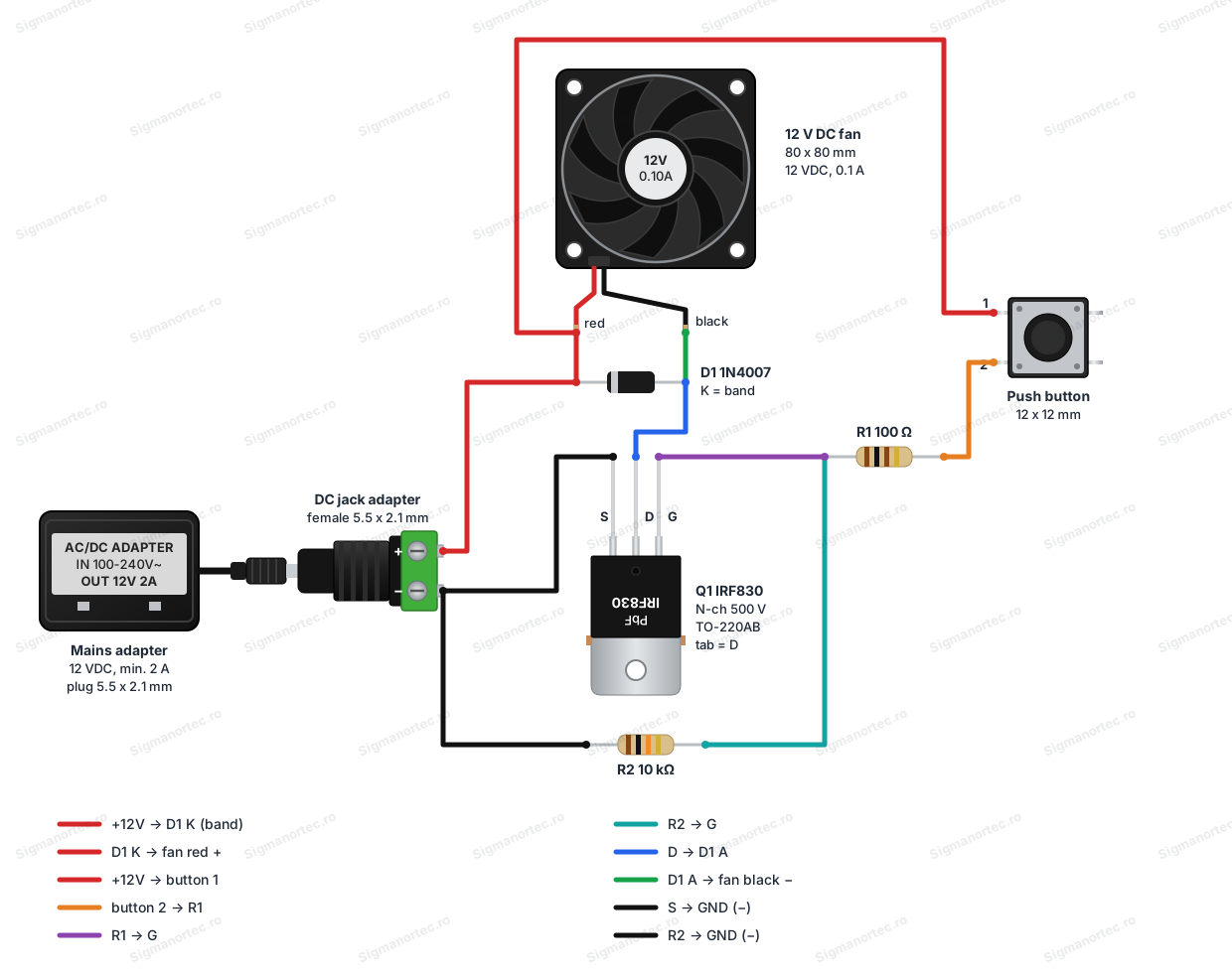
In this circuit, the fan is connected between +12 V and the drain, meaning the transistor switches on the ground side of the load. When we press the button, the gate receives 12 V through R1 of 100 Ω. R2 of 10 kΩ stays connected between the gate and the source, so the actual gate voltage is 12 V × 10 kΩ / 10.1 kΩ, which is approximately 11.9 V. This value is above the 10 V point and below the limit of ± 20 V.
R1 limits the charging current of the gate and dampens oscillations. With Ciss of approximately 610 pF, the time constant is 100 Ω × 610 pF = 61 ns. The total gate charge is at most 38 nC, so the complete switching takes at most a few microseconds, which is practically instantaneous for a fan. When we release the button, R2 discharges the gate towards the source and the transistor turns off. Without R2, the gate capacitance would remain charged and the fan would keep running.
Conduction losses are calculated with P = I² × RDS(on). For the 0.1 A fan we get 0.1² × 1.5 = 0.015 W, so no heatsink is needed. At 1 A the loss reaches 1.5 W. The voltage drop across the transistor, when it is on, is at most 0.1 A × 1.5 Ω = 0.15 V.
The fan is an inductive load. When the transistor turns off, the motor coil generates a voltage spike. The 1N4007 diode placed in parallel with the fan, with the cathode (band) at +12 V and the anode at the drain, absorbs this spike and protects the transistor.
Connection:
Use a 12 VDC mains adapter, minimum 2 A, with a 5.5 x 2.1 mm female DC jack adapter with + and - screw terminals. Do not touch the mains side of the adapter, and make all connections with the adapter unplugged from the socket. The circuit works at 12 V, so no level converter is needed. Looking at the IRF830 with the printed side facing you and the pins pointing down, the pins from left to right are: 1 = G, 2 = D, 3 = S. The metal tab is connected to the drain.
| Product pin | Connected to | Role |
|---|---|---|
| G (pin 1) | Leg 2 of the button through R1 of 100 Ω, plus R2 of 10 kΩ to the source | Control gate. R1 limits the charging current, R2 keeps it at 0 V when the button is released |
| D (pin 2) | The black wire of the fan and the anode of the 1N4007 diode | Drain, switches the ground side of the load |
| S (pin 3) | The - terminal of the adapter and the free end of R2 | Source, common ground of the circuit |
| Metal tab | Not connected to anything | Electrically connected to the drain, do not touch it when the circuit is powered |
The rest of the circuit is wired as follows: the + terminal of the adapter goes to leg 1 of the button, and from here to the red wire of the fan and to the cathode of the 1N4007 diode (the end with the band). Leg 2 of the button goes to R1. For a button with four legs, use the multimeter in continuity mode to find the pair of legs that connect only while the button is pressed, and use that pair.
Configuration:
The circuit has no programming. The component values are chosen as follows. R1 of 100 Ω can be replaced with any value between approximately 47 Ω and 470 Ω without changing the operation with a small load. R2 can be from 10 kΩ up to 100 kΩ. A lower value discharges the gate faster, but draws more current from the adapter when the button is pressed. The gate voltage must never exceed ± 20 V.
For other loads, check the current. At 0.1 A, the IRF830 works without a heatsink. As the current rises towards 1 A, the loss reaches 1.5 W and the transistor heats up strongly, so use a heatsink. Insulate the tab from it and from the enclosure, because the tab is at the drain potential. The absolute limit is ID = 4.5 A at TC = 25 °C and 2.9 A at TC = 100 °C, with VGS = 10 V.
| Parameter | Value in the circuit | Allowed range |
|---|---|---|
| R1 (gate) | 100 Ω | 47 - 470 Ω |
| R2 (gate-source) | 10 kΩ | 10 - 100 kΩ |
| VGS with the button pressed | approximately 11.9 V | 10 - 12 V recommended, maximum ± 20 V |
| Fan current | 0.1 A | Heatsink recommended towards 1 A, maximum 4.5 A at TC = 25 °C |
Usage example:
Wire the circuit with the adapter unplugged from the socket. Step 1: insert the IRF830 on the breadboard with the printed side facing you and identify the pins G, D, S from left to right. Step 2: connect R2 of 10 kΩ between G and S. Step 3: connect R1 of 100 Ω between G and leg 2 of the button. Step 4: connect S to the - terminal of the adapter.
Step 5: connect the black wire of the fan to D. Step 6: connect the red wire of the fan to leg 1 of the button and to the + terminal of the adapter. Step 7: mount the 1N4007 diode with the anode at D and the cathode (band) at the red wire of the fan. Check the orientation of the diode once more, then plug the adapter into the socket.
Press the button and keep it pressed: the fan starts. Release the button: the fan stops, because R2 discharges the gate. If you have a multimeter, measure the voltage between D and S. With the button pressed you should get at most approximately 0.15 V, and with the button released approximately 12 V. Also measure the voltage between G and S: approximately 11.9 V with the button pressed and 0 V with the button released.
Common problems:
The fan does not start when you press the button. The most likely cause is the wrong order of the pins or of the connections. Check that G is pin 1, D is pin 2 and S is pin 3, looking at the transistor with the printed side facing you and the pins pointing down. Then measure the voltage G - S with the button pressed, which should be approximately 11.9 V. If it is 0 V, the button does not close the contact and you must choose another pair of legs.
The fan runs continuously or stays on after you release the button. The cause is the missing or poorly contacted resistor R2, which leaves the gate undischarged. Check R2 between G and S. If R2 is correct, the transistor may be defective (short circuit between D and S) after an overload or a diode mounted in reverse.
The fan turns weakly or slowly, and the transistor heats up. The gate does not receive enough voltage and the transistor is only partially open. Measure VGS, which must be 10 - 12 V. Check the adapter and the values of R1 and R2.
The adapter shuts down through protection or heats up when the button is pressed. The 1N4007 diode is probably mounted in reverse and is short-circuiting the supply through the transistor. Unplug the adapter from the socket and check that the diode band is towards +12 V, and the anode towards the drain.
The transistor heats up with a small fan. Check the real current of the fan, which should be around 0.1 A, and the gate voltage. A high current or a gate drive below 10 V increases the losses.
Limitations and tips:
The IRF830 is designed for high voltages, up to 500 V, but its on-state resistance of maximum 1.5 Ω is high for high-current loads at 12 V. For such loads, choose a MOSFET with a much lower RDS(on) that can be driven directly from the available voltage.
The value of 4.5 A is valid when the case temperature is kept at 25 °C, which requires an efficient heatsink. At 1 A, the loss of 1.5 W and the junction-to-ambient thermal resistance of maximum 62 °C/W lead to a temperature rise of over 90 °C, so for continuous operation use a heatsink earlier.
Do not exceed ± 20 V on the gate, and handle the transistor with anti-static protection. For inductive loads, always mount the protection diode.
After this circuit you can control other DC loads, for example an LED strip, a relay or a small pump, with the same gate network, respecting the maximum current and the heatsink. For dangerous voltages or mains voltage, work only with proper insulation and by a qualified person.